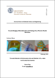
Khan, Saleem (2016) Towards Merging of Microfabrication and Printing of Si µ-Wires for Flexible Electronics. PhD thesis, University of Trento.
| PDF - Doctoral Thesis 4Mb |
Abstract
This PhD thesis focuses on the investigation and development of a feasible technology route for fabricating multifunctional flexible electronic devices through heterogeneous integration of organic/inorganic materials on polymeric substrates. The three types of printing technologies investigated during this research include: (a) Transfer printing of inorganic semiconductors processed through standard microfabrication techniques, (b) Spray coating for deposition of organic dielectrics and metal patterns, and (c) Screen-printing of solution based transducer materials. Fabrication of electronic devices based on transfer printing of high-mobility inorganic semiconductor materials (i.e. Si), aided by high-resolution possible with microfabrication technology, was explored for high performance electronics. A cost-effective processing of printable materials is desired and therefore, through printing technologies, this thesis also explored ways to bring closer the well-established microfabrication and conventional printing tools. Due to commercial interests, the major research focus in flexible electronics thus far has been on applications such as photovoltaics and displays. However, this research is focused on active/passive electronics for sensing applications like electronic skin, which is of significant interest in robotics for safe human-robot interaction and other manipulation and exploration tasks. Optimization of the Transfer Printing for translating Si microwires from SOI (silicon on insulator) wafers on secondary flexible substrates has been investigated. Processing steps have been improved for fabrication of Si microwires on donor wafers and dry transferring them onto flexible PI (polyimide) and PET (polyethylene terephthalate) substrates. The downscaling of Si in the form of microwires and using them as building block for active devices such as field effect transistors were explored in this thesis. The microwires retain the high carrier mobility, robustness, high performance and excellent stability. Arrays of MISFETs (metal insulator field effect transistors) structures were successfully fabricated and the response variations were compared. The differently doped Si microwires were analyzed in an asymmetric metal semiconductor metal (MSM) structures under planar and bend mode conditions. The optical response as well as the thermoelectric properties of the alternately doped pn-Si microwires were also investigated. A feasible fabrication route is presented, where combination of transfer printing for Si microwires and development of the subsequent post-processes by additive manufacturing techniques i.e. Screen-printing, Spray coating and Micro-spotting are mainly investigated. The Si microwires are employed as the semiconductor in the MISFET devices whereas screen-printed metal patterns are used for back-gate and deposition of dielectric layer is performed through spray coating. In parallel, screen-printing is also used for development of large area pressure sensor patches using two different materials i.e. P(VDF-TrFE) (Polyvinylidene Fluoride Trifluoroethylene) and nanocomposites of MWCNTs/PDMS (multiwall carbon nanotubes mixed with poly(dimethylsiloxane) for measuring dynamic and static contact events. Promising results have been achieved by developing a cost-effective way of manufacturing an all Screen-Printed flexible pressure sensors using piezoelectric transducer through P(VDF-TrFE) and piezoresistive based MWCNT/PDMS nanocomposites. Active electronic circuitry is needed for signal conditioning, amplification or processing of the sensory data on the flexible foils, which is deemed to be developed through Si microwires based technology in the next phase of the project. Ultimate goal of the PhD study was to develop a fabrication platform by combining three different printing technologies for large area sensor patches. Major challenges involved in the development of flexible device designs and printing technologies are highlighted and addressed with dependable solutions. The research concludes with proposing an innovative approach towards heterogeneous integration of large area sensory cells made of organic materials to the active devices based on inorganic semiconductors such as Si microwires. This technological platform for heterogeneous integration of devices made of diverse materials (organic, inorganic etc.) on soft substrates is believed to be a step-change needed to advance flexible electronics towards manufacturing.
| Item Type: | Doctoral Thesis (PhD) |
|---|---|
| Doctoral School: | Materials Science and Engineering |
| PhD Cycle: | 28 |
| Subjects: | Area 09 - Ingegneria industriale e dell'informazione > ING-IND/22 SCIENZA E TECNOLOGIA DEI MATERIALI |
| Repository Staff approval on: | 09 Mar 2016 11:59 |
Repository Staff Only: item control page


